
RECOMMENDATIONS AND TECHNICAL CAPABILITIES
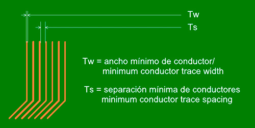
The limitations for width and separation between conductors depends on the based copper. The table below sums up the manufacturing options:
External layers
| Copper base* | Minimum width (Tw) | Minimum gap (Ts) |
|---|---|---|
| 18µ | 0.125mm | 0.125mm |
| 35µ | 0.200mm | 0.200mm |
| 70µ | 0.250mm | 0.250mm |
Internal layers
| Copper base | Minimum width (Tw) | Minimum gap (Ts) |
|---|---|---|
| 18µ | 0.110mm | 0.110mm |
| 35µ | 0.125mm | 0.125mm |
| 70µ | 0.250mm | 0.250mm |
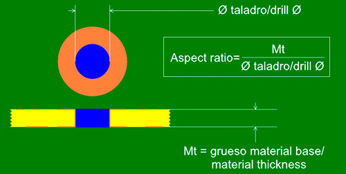
The most important characteristics of the drills on the printed circuit board are: diameter, if they are plated or non plated and their depth. The last characteristic is determined by the thickness of the base material, and is key in determining the minimum drill possible as described in the calculation section.
Minimum annular rings
| Drilling type | Minimum drilling diameter |
|---|---|
| Plated | 0.200mm |
| Non plated | 0.300mm |
| Blind via | 0.500mm |
Final diameter tolerances
| Drilling type | Tolerance |
|---|---|
| Plated | +0.1mm/-0.05mm |
| Non plated | +0.1mm/-0.05mm |
Calculate Aspect Ratio:
The Aspect Ratio is the relationship between the minimum manufacturable drilling on the thickness of the circuit board, following the formula below:
![]()
Aspect ratio ≤ 6.
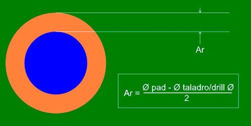
The annular ring is the metal ring left around the drilling on a pad.
Minimum annular ring
| Plated | Minimum annular ring (Cm) |
|---|---|
| Cu Base+18µ | 0.100mm |
| Cu Base+35µ | 0.200mm |
Internal layers
| Plated | Minimum annular ring (Cm) |
|---|---|
| 18µ , 35µ , 70µ | 0.150mm |
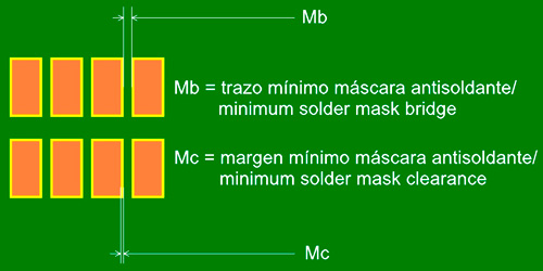
The solder mask is a coating put on to protect the printed circuit board, so that it cannot be soldered on except in designated areas.
| Colour | Minimum margin (Mc) | Minimum width (Mb) |
|---|---|---|
| Green | 0.075mm | 0.100mm |
| White, black, grey, blue, red | 0.075mm | 0.150mm |
Note: except when otherwise specified, the mask will be adapted by eliminating traces smaller than the minimum trace and expanding it to the minimum margin.
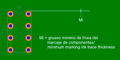
Used to reference the components and indicate their position and dimensions on the printed circuit board, can also include logos, circuit board codes, quality marking and any images that comply with the minimum parameters for production capacity.
| Colour | Minimum width (Mi) | Minimum trace margin/soldermask (Mt) |
|---|---|---|
| White | 0.125mm | 0.100mm |
| Black | 0.180mm | 0.100mm |
Note: except when specified otherwise, all marking images coinciding with areas without solder mask will be eliminated.
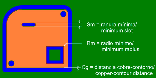
CNC milling is an automatic cutting system that uses a rotating tool guided by a numerical control system. The mechanical options for milling done with this process are determined by the precision of the numerically controlled machine and the diameter of the tool used, the latter being the only variable the designer may change.
Mechanical options
| Concepts | Figures |
|---|---|
| Minimum tool diameter (Sm) | 0.80mm |
| Minimum radius for internal windows (Rm) | 0.40mm |
| Position tolerance | +/-0.20mm |
| Minimum Copper-Edge gap (Cg) | 0.20mm |
Plated Edges/Castellated holes (half holes)
Type of process used to connect circuit boards. It consists in putting a metallic cover on the sections at the edge of the circuit board to allow for lateral soldering and electric union between layers.
Plated Edges
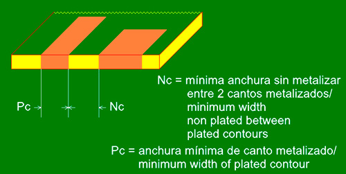
| Concepts | Figures |
|---|---|
| Minimum legth (Pc) | 1.50mm |
| Minimum separation between lengths (Nc) | 0.80mm |
| Position tolerance | +/-0.20mm |
| Size tolerance | +/-0.10mm |
Castellated holes (half holes)
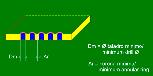
| Concepts | Figures |
|---|---|
| Minimum drill (Dm) | 0.80mm |
| Minimum annular ring (Ar) | 0.20mm |
| Minimum separation between pads | 0.20mm |
| Position tolerance drill/edge | +/-0.20mm |
| Size tolerance | +/-0.10mm |
Bevelling
Type of mechanisation used to facilitate insertion of circuit boards into card-type connectors (e.g. PCI, AGP, ISA, etc.). This reduces the edge of the circuit board where the connector is located to 30°.
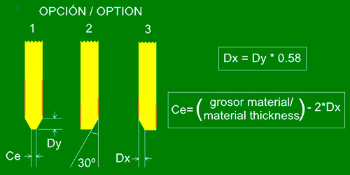
Note: this process affects the whole length of the edge of the circuit board where the connector will be located, even if it doesn’t take up the whole length. This process should not be used on top of the metallic area of a circuit board, so it is recommended to apply the following formula:
![]()
Conical Countersink
Type of process used to embed the head of screws with a cone shape. It is a 45° groove drill on one of the sides of the circuit board.
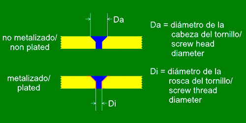
Note: the maximum upper diameter (Da) is determined by the following formula:
![]()
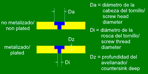
Flat Countersink
Type of process used to embed the head of screws with a flat shape. It is a 90° groove drill on one of the sides of the circuit board.
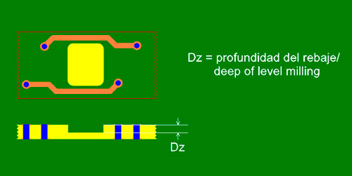
Grooves
Process required to assemble certain types of components such as contactors, joysticks onto the PCB or for components that cannot stick out above the surface of the PCB, membrane keyboards for example.
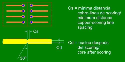
Scoring or V-cut consists in creating two grooves in a V shape on either side of the circuit board coinciding with the axis that divides them. The hold force between the circuit boards is determined by the size of the core left between the two V-cuts.
Applicable figures
| Concepts | Figures |
|---|---|
| Minimum material thickness | 0.50mm |
| Maximum material thickness | 2.40mm |
| Position tolerance | +/-0.10mm |
| Minimum separation between Copper – Edge (Cs) | 0.40mm for base material thickness 0.8mm 0.50mm for base material thickness 1.6mm 0.70mm for base material thickness 2.4mm |
| Slot angle | 30º |
Note: Recommended use of V-cut depaneling machine. After separating the circuit boards, the absolute measurements of the circuit boards may vary +/- 0.30 mm.